A few weeks ago, a memory popped up on my phone of a 3-bit added I had made from purely transistors and resistors. I remember building this after being fascinated by how computers could take electric charges and use clever circuitry to turn these into complex mathematical computations. After seeing went to watch a quick video to remind me of the logic behind this, and I really got in a rabbit hole.
After watching a few video series, mainly Ben Eater’s breadboard computer, I was really inspired to take up a challenge of my own, something that would really force me to truly understand the low-level behavior of a basic computer.
Over the next few weeks and months, I intend to build a prototype calculator and then a basic programmable computer from transistors alone. Due to obvious cost issues, I am going to design it on Logisim first.
Plan:
- Start off with building a basic adder. This will start with a value, store it in memory, take a new value, add it to the total and then store the new total. This will familiarise me with basic memory and logical arithmetic.
- The I want to go onto build a really basic programmable computer, that can loop, retrieve values from memory address.
- The dream for me to write a VERY basic programming language with a compiler such that I can code to this computer
Rules:
- Apart from when it is truly necessary, I will try and stop myself from using designed logic circuits for cmponents. Obviously, all I am doing has been done before, but I would like to try and work it out for myself. My plan is to design my own and then research to see how I could improve my design. This is with the exception of full adders and D-latches which I already knew upon starting the project.
Progress
I will post the basic principles here as it helps me learn to explain it, and in case this gets far enough that people want to immitate it.
Addition
If you are reading this blog, I am guessing you are familiar with how to store numbers in binary. I am guessing you are also familiar with ‘long addition’, or at least have some vague memory of it from primary school. When combining these two ideas it allows you to add numbers using binary.
Inside a computer you can store and send individual bits using electricity. A high current (on) can be interpretted as that bit storing a value of 1. Low or no current stores the opposite. A computer can therefore perform long addition by checking for two high currents, and then carrying this current to the next bit if they are both high. This is performed by a a circuits called half and full adders.
A half adder is the most basic form of computer arithmetic. It can only be used for adding 1 bit.
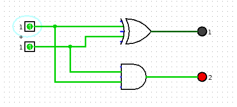
If you want to compute calculations with numbers greater than 1, which I’m guessing you do, you need to use a full addder. This uses the half adder for the first bit, and then if both bits are on, it carries the 2 to the next adder. The full adder has the capability if see if a 1 was carried from the last bit and encorporating thay into its sum.
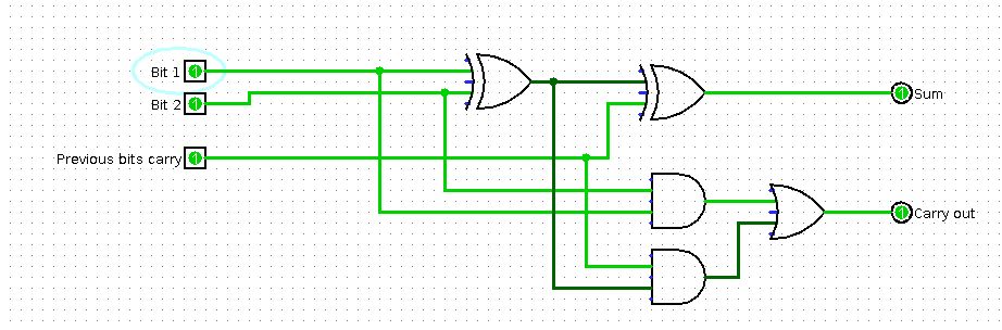
These full adders can be stacked on top of one another, connect the carry in and out pins, to allow us to add arbitrary length numbers.
Memory
In order us to perform calculations that required more than step to compute, we must have a way to store the values between calculations. To do this, a logic circuit known as D-latch is used. This allows us to store a singular bit of information using logic gates.
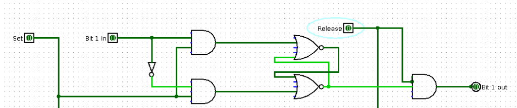
When the set pin is high, it will store whatever value is in the bit in pin, even after the set pin is off. This allows us to store one bit! In order to store more bits, I just put these D-latches in parallel. The set and release pins activate all the D-latches, so that byte or nibble of information can be written or accessed.
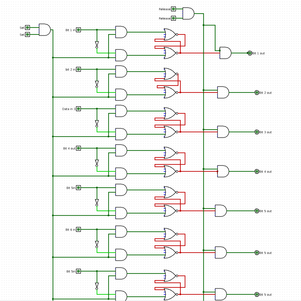
One of my favorite features of Logisim is that it allows you to make chips out of these logic circuits. The above circuit can be turned into a simple memory chip.
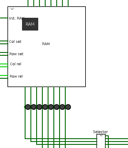
Now we have a way to store information, we need a way of reading and writing to a variety of memory addresses. This is Random Access Memory. The RAM I designed is below:
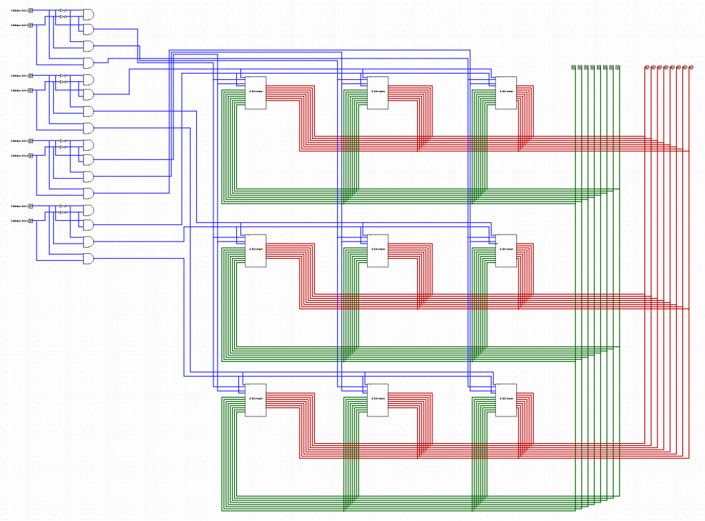
I will break it down part by part. In order to access a ‘memory address’ we need a way of taking a binary number and then using that number to either read or write to a specific byte of memory. This is done by using a grid system. As shown earlier, each byte of memory requires two positive currents to either be written or have its data released. Each one of these write and set pins is connected to both a row and column wire. The write or release mode will only be acted when both its row and column are activated. The next step for the RAM is to be able to toggle between read and write.
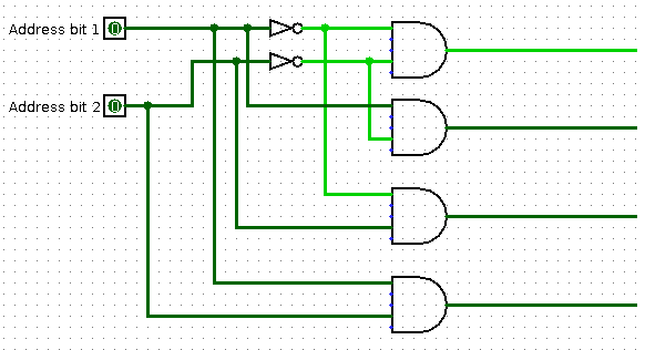
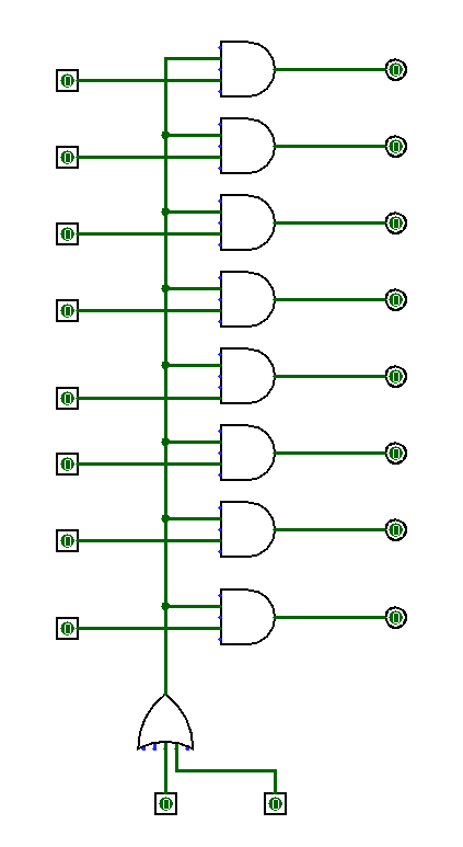
In order to turn the binary address into the byte actually being activated, a binary to unary converter was made. This will take the number N in binary and then activate the Nth pin. To do this you set up and gates for every possible value, and hard wire in which bits should be on or off
Update
I have made a lot of progress since last posting The RAM now works! It can take a memory address, write data to it and then store it. It can then retrieve the data from that memory address at a later time. I’ve added a video of it working below.
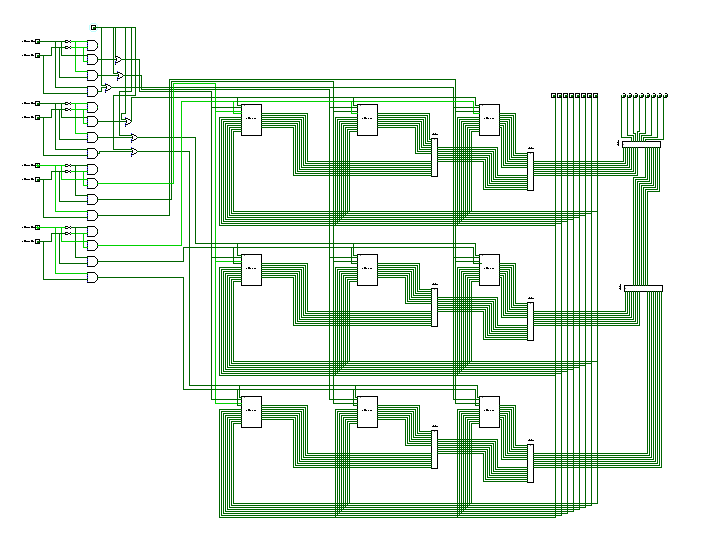
If you compare to the image above, two parts have been added. Firstly, an initiate pin has been added. This is to prevent errors at the start of the simualtion within the bits being neither ones of zeros. Powering this pins sets all pins to 0. Secondly, I had to add a chip I made called a ‘linker’. Logisim has a feture I find slightly irritating in which if you write a 0 and 1 to a wire at the same time it gives you an error. In real life, a low current and a high current simply equals a high current, so it an unneeded level of complexity in my opinion. Anyway, a linker is simply a circuit filled with OR gates to link to two wires, which has the same effect as joining them up normally.
CPU
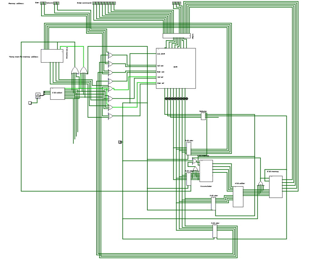
I have also begun work on the programmable computer. This added a LOT of complexity but I will do by best to describe how it works.
I have not yet tested it properly, as I still want to make a very basic compiler and need to find a way to write to the RAM externally.
A brief overview of how it works:
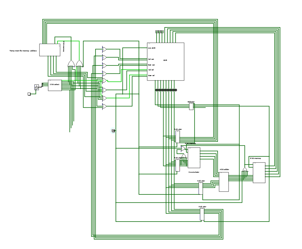
The RAM can store 9 bytes of data. Each byte it manually split into two sections, first 3 bits are for command, next 5 bits are for values. This value is normally a memory address.
The program is stored in the first bytes of the RAM. In its current state, the program can be a maximum 4 bytes. I said it was basic. The CPU has 3 commands:
- READ: this is when the first 3 bits are 001. The next bit is free in this case, then the next 4 bits are for memory address. This memory address ca be broken down into two parts. The first two bits are for column of the data and the next two bits are for the row. Howevere, this command cannot be used instantaneous the read address pins of the RAM are still be used by the ticker (I will explain later). It therefore stores the memory address in the 5-bit memory at the top left of the screen. It is then read from on the next tick. This is a work around and I want to find a way to improve upon this in the future.
- ADD: this is the 010 command. It is followed by 5-bits of what number to add. This will add this number to what ever number is stored in the actuator at the bottom right.
- WRITE: this is the 011 command. It is followed the memory address of where you want to write to. It can be done instantaneously as the write pins are not being used.
How to turn binary into commands?
To turn the first 3 bits into commands the computer can execute, I made a chip I called the ‘selector’. This is the same as the binary to unary converter. If it gets N in binary, it will turn on the Nth output of the chip. These outputs are then hardwired to another chip I added I called an ‘activator’. This chip is essentially a multi-input, multi-output transistor. It can activate up to 8 connections at once. It is shown below.
If wired correctly you can link together the correct parts of the CPU at the correct time, you can achieve all three commands.
Quick overview of connection:
- READ: links together the last 4 bits with the address cell and activates the write setting of that memory cell. The next tick will then activate the reading, which in turn will activate the write setting of actuator memory cell, such that it can store the whatever is at that address close to the CPU.
- ADD: this turns on the pin which releases the accumulator memory (the value which has been loaded from the RAM) into the first 4 bits of the binary adder. It also connects together the last 5-bits of the RAM output with the bottom 4 bits of the adder. The output is then store in a temporary memory cell.
- WRITE: as all we are currently doing is adding, this releases the value stored as the result of the adding and writes it back to memory using the given memory address.
This CPU hasnt been tested yet, as I currently need to code it by hand in binary, but I hope to soon make a very basic compiler so that I can write to it.
Going through commands
In the left middle you will see a counter joined to a 3 bit selector. This counter is the only chip that I didnt make from logic gates as it is quite complex. The CPU workers on a manual ticker, that ticks everytime you press the button connected to it. This is then counted by the counter which outputs the count is binary, before resetting at after 7. After the counter, I hardwired each count to read from a specific memory address. I also added a gap into between each memory read to allow the circuit to decode and execute instructions.
UPDATE: It is programmable!
I added some binary inputs in the top left so you can manually type binary to a set of memory addresses! I call that programmable!
UPDATE: NEW CPU DESIGN
Unsurprisingly, the CPU turned out to be pretty bad. It could run the programmed but crashed so often I have decided to design the CPU with some added functionality.
So far I have only redone the read command with an added function. The 4th bit is now used to say which of the newly added registers you want the value at that memory address written to.
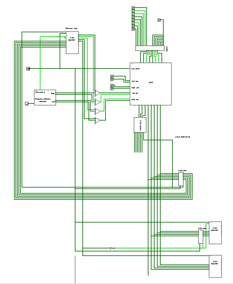
This CPU has one function. It can retrieve values from memory address and either write them to register 0 or register 1.